Quantinuum Finalizes $100 Million CHIPS Funding Agreement
Sep 08, 2026
Chips
Uviquity announced in a press release the launch of a chip-scale laser operating at 229 nanometers, the first of its kind produced from a single semiconductor chip. The device provides collimated, narrow-linewidth ultraviolet output for analytical and inspection uses across several industries.
The laser is built on Uviquity's aluminum nitride photonic integrated circuit platform, which generates deep ultraviolet light through second harmonic generation in proprietary waveguides. The company holds over twenty pending patents related to the design, which was first presented at SPIE Photonics West in January 2026.
Sampling for original equipment manufacturer partners will begin in the fourth quarter of 2026. Target applications include semiconductor inspection, pharmaceutical and petrochemical process monitoring, environmental sensing, and defense detection systems. The compact form factor supports handheld and embedded instrument designs that operate on low-voltage electrical input.
The same platform is being developed for far ultraviolet disinfection products intended for air, water, food, and medical use, enabling Uviquity to serve both sensing and disinfection markets from a single semiconductor architecture.
Consider subscribing to one of our newsletters like Silicon Brief or Daily AI Brief.
Also, consider following us on social media:
Weekly coverage of AI hardware developments including chips, GPUs, cloud platforms, and data center technology.

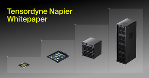
 Tensordyne
This Tensordyne whitepaper presents Napier, an inference-focused AI processor and rack-scale system based on the company’s TDN Math logarithmic number system. It examines infrastructure requirements for large mixture-of-experts and agentic models, compares major inference architecture approaches, and details the TDN AIP processor, TDN72 pod, TDN Link fabric, and Napier Ultra configuration. The paper reports simulation-based performance, cost, and accuracy-validation results, including Tensordyne’s projected comparison of one Napier rack with a nine-rack Nvidia Rubin plus Groq deployment; the chip is reported as taped out and in fabrication.
Read moreDaily AI Brief: the AI news that matters, in your inbox.