MiTAC Shows Liquid Cooled AI Infrastructure at OCP Summit
Oct 12, 2026
Chips
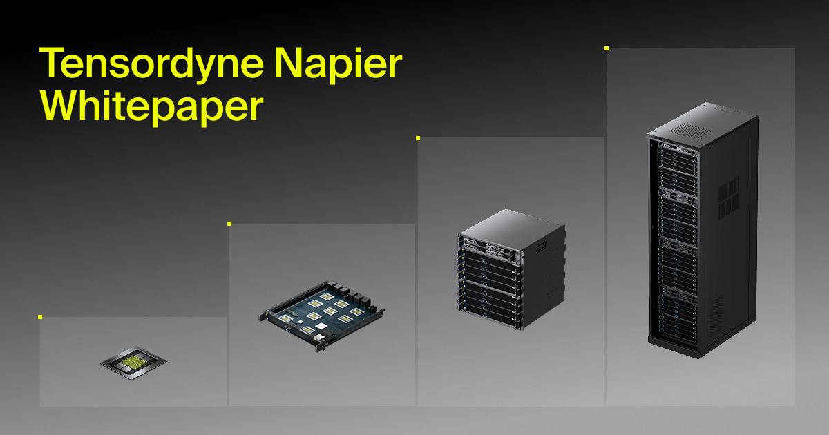
Tensordyne has detailed its Napier AI inference chip and data center system in a company whitepaper. The system combines logarithmic arithmetic, large on chip SRAM, HBM3e memory, and a low latency scale up fabric, and the company says the chip has taped out and is in fabrication.
The TDN AIP processor provides 2.11 PFLOPS of FP8 dense compute, 256 MB of SRAM, 144 GB of HBM3e, and 1 TB per second of scale up bandwidth. A TDN72 pod contains 72 processors, 10.4 TB of HBM, and 68.8 TB per second of scale up bandwidth while operating at 30 kW. Tensordyne says four pods can fit in a 52 rack unit cabinet and provide 608 PFLOPS of FP8 dense compute at less than 120 kW.
Napier uses the company's TDN Math, a logarithmic number system that replaces multiplication with addition. Tensordyne says it is the first company to fully productize a logarithmic number system for AI inference and claims the approach cuts compute area by about three times and compute power by about five times while retaining model accuracy. An earlier 7 nm prototype implemented the original version, and the company says it has validated accuracy through bit accurate emulation across language, mixture of experts, image, audio and video models.
The headline claim is that one Tensordyne rack could do the work of nine. In the whitepaper the company compares a single TDN rack with a nine rack Nvidia Rubin plus Groq configuration on a 2 trillion parameter mixture of experts model, and projects about 1,300 tokens per second per user at about $11 per million tokens in its high speed mode, against 800 tokens per second per user at about $150 per million tokens for the Nvidia and Groq combination. Those figures come from Tensordyne's internal modeling and have not been independently verified.
The processor is built on a 3 nm process from TSMC. The TDN72 pod is assembled from system components supplied by Hewlett Packard Enterprise's Juniper business, and a multi pod version called Napier Ultra connects up to 16 pods through Layer 2 switches such as those based on Broadcom Tomahawk Ultra. In a LinkedIn post announcing the whitepaper, the company said: "Chip is taped out with Broadcom and in wafer fab on TSMC 3nm" and "System bring-up of compute tray with HPE Juniper scale-up fabric is ahead of schedule". Tensordyne says all published performance and cost figures are based on modeling and simulation pending verification with production silicon.
Consider subscribing to one of our newsletters like Silicon Brief or Daily AI Brief.
Also, consider following us on social media:
Weekly coverage of AI hardware developments including chips, GPUs, cloud platforms, and data center technology.

.png)
 Thomson Reuters
This report by Thomson Reuters explores the integration and impact of generative AI technologies, such as ChatGPT and Microsoft Copilot, within the professional services sector. It highlights the growing adoption of GenAI tools across industries like legal, tax, accounting, and government, and discusses the challenges and opportunities these technologies present. The report also examines professionals' perceptions of GenAI and the need for strategic integration to maximize its value.
Read moreDaily AI Brief: the AI news that matters, in your inbox.